

CP Series Step Instrument
The step instrument is an advanced micro-nano measuring instrument with independent intellectual property rights owned by Zhongtu Instrument. The instrument adopts core technologies such as sub-angstrom resolution displacement sensors, ultra-low noise signal acquisition, ultra-fine motion control, and calibration algorithms, and has excellent performance.
Keywords:
Electronics and Electrical Engineering
Dimension measurement
Product Attachments:
Retail Price
Market Price
Weight
Category:
Remaining Stock
隐藏域元素占位
- Product Description
-
- Commodity name: CP Series Step Instrument
The step instrument is an advanced micro-nano measuring instrument with independent intellectual property rights owned by Zhongtu Instrument. The instrument adopts core technologies such as sub-angstrom resolution displacement sensors, ultra-low noise signal acquisition, ultra-fine motion control, and calibration algorithms, and has excellent performance.
Product Introduction
The Step Profiler is an advanced micro-nano measuring instrument with independent intellectual property rights owned by Zhongtu Instrument. The instrument adopts core technologies such as an angstrom-level resolution displacement sensor, ultra-low noise signal acquisition, ultra-fine motion control, and calibration algorithms, and has excellent performance.
The Step Profiler is widely used in: universities, research laboratories and institutes, semiconductors and compound semiconductors, high-brightness LEDs, solar energy, MEMS microelectromechanical systems, touch screens, automobiles, and medical equipment.
The Step Profiler uses contact surface topography measurement, a new development in traditional surface topography measurement. It has extremely low contact force and does not have special requirements for the reflectivity, material type, or hardness of the measured surface. It has a very wide range of sample adaptability, high data reproducibility, stable and convenient measurement, and high efficiency. It is a widely used micro-nano sample measurement method in microscopic surface measurement.
Typical Applications
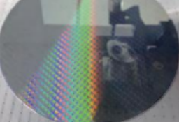

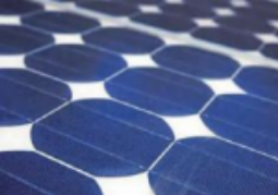
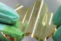
Semiconductor Applications Large Substrate Applications Glass Substrate and Display Applications Flexible Electronic Device Thin Film Applications Step Height of Deposited Thin Films Printed Circuit Boards (protrusions, step height) AMOLED Organic Photodetectors Step Height of Resist (Soft Film Material) Window Coatings Step Height Measurement in LCD Screen Development Organic Thin Films Printed on Films and Glass Etch Rate Determination Wafer Masks Touch Panel Thin Film Thickness Measurement Touch Screen Copper Traces Chemical Mechanical Polishing (corrosion, pitting, bending) Wafer Chuck Coatings, Polishing Plates Solar Cell Coating Thin Film Measurement Technical Parameters and Environmental Requirements
Product Model
CP200
Measurement Technology
Probe-based surface profilometry
Sample Observation
Optical navigation camera: 5-megapixel high-resolution color camera, FoV, 2200*1700μm
Probe Sensor
Ultra-low inertia, LVDC sensor
Measuring Force
1-50mg adjustable
Probe Selection
Probe radius of curvature 2μm, angle 60°.
Platform Travel Range X/Y
Electric x/y (150mm*150mm) (manually levelable)
Sample R-9 Stage
Electric, 360° continuous rotation
Single Scan Length
55mm
Maximum Sample Thickness
50mm
Maximum Wafer Size on Stage
150mm (6 inch), 200mm (8 inch)
Step Height Repeatability
5Å, range 330μm / 10Å, range 1mm (measuring 1μm step height, 15 times)
Sensor Range*1
330μm or 1mm
Vertical Resolution
Resolution <0.01Å (at 13μm range)
Scanning Speed
2μm/s-10mm/s
Dimensions (LxWxH) mm
640*626*534
Weight
40kg
Instrument Power Supply
100-240VAC, 50/60Hz, 200W
Operating Environment
Relative Humidity: Humidity (no condensation) 30-40%RH Temperature: 16-25℃ (temperature change less than 2℃ per hour)
Ground vibration: 6.35μm/S (1-100Hz) Audio noise: ≤80dB Airflow: ≤0.508 m/S (downward flow)
Previous Page
Product Inquiry
Welcome to Xiamen Jingwei Instrument Equipment Co., Ltd. Official Website
If you are interested in our products and services, please contact us or leave us a message, and we will be happy to serve you.
Company Address:
(Domestic ):Room 3F-D2, North Rongxin Building, Huli District, Xiamen
(Vietnam ): No. 388, Nguyen Huu Tien Residential Area, Dong Van Ward, Duy Tien Town, Ha Nam Province, Vietnam.
Tel:+86 0592-5631009(Domestic)
Mobile:+86 13859953392(Domestic)
Email:dong5631009@126.com
Tel:+84 0384656346(Vietnam)
Mobile:+84 0384656346(Vietnam)
Email:dongjinzhen9@gmail.com
Quick Navigation:

Mobile Website
Website Construction:www.300.cn | TAG | Privacy policy