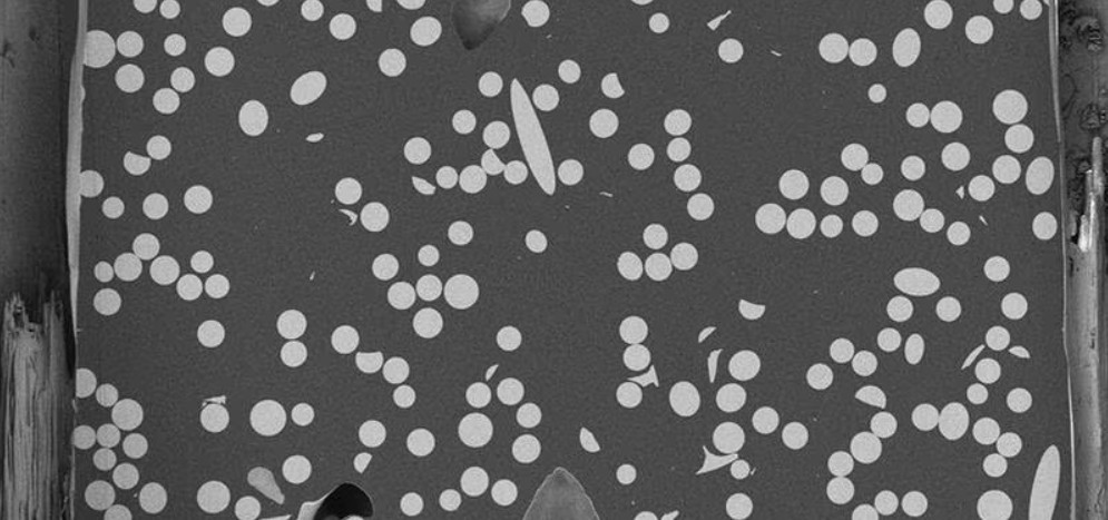
Silver particles on silicon dioxide


Scanning electron microscope Thermo Apreo 2 SEM
The Apreo 2 high-resolution field emission scanning electron microscope boasts superior low-voltage, low-beam current imaging capabilities. It comes standard with six detector types (T2, T2, T3, ETD, Nav-Cam, IR-CCD). A nanometer-scale response rate minimizes electron beam dwell time, and various intelligent scanning technologies minimize electron beam damage to the material. Optimized for the characterization and analysis of lithium battery materials, it enables high-precision analysis of the particle size, shape, and composition of micro- and nanostructures.
Keywords:
Microscope
Electronics and Electrical Engineering
Product Attachments:
Retail Price
Market Price
The Apreo 2 high-resolution field emission scanning electron microscope boasts superior low-voltage, low-beam current imaging capabilities. It comes standard with six detector types (T2, T2, T3, ETD, Nav-Cam, IR-CCD). A nanometer-scale response rate minimizes electron beam dwell time, and various intelligent scanning technologies minimize electron beam damage to the material. Optimized for the characterization and analysis of lithium battery materials, it enables high-precision analysis of the particle size, shape, and composition of micro- and nanostructures.
Weight
Category:
Quantity
-
+
Remaining Stock
隐藏域元素占位
- Product Description
-
- Commodity name: Scanning electron microscope Thermo Apreo 2 SEM
The Apreo 2 high-resolution field emission scanning electron microscope boasts superior low-voltage, low-beam current imaging capabilities. It comes standard with six detector types (T2, T2, T3, ETD, Nav-Cam, IR-CCD). A nanometer-scale response rate minimizes electron beam dwell time, and various intelligent scanning technologies minimize electron beam damage to the material. Optimized for the characterization and analysis of lithium battery materials, it enables high-precision analysis of the particle size, shape, and composition of micro- and nanostructures.
Product Overview:
The Thermo Scientific Apreo 2 SEM field emission scanning electron microscope is equipped with real-time elemental imaging and an advanced automated optical system, enabling the resolution of gray areas and freeing you from concerns about microscope performance, allowing you to focus more on your research.
Focus more on the research itself.
The Thermo Scientific Apreo 2 SEM offers versatility and high-quality imaging performance. It adopts an innovative final lens design, introducing an electrostatic final lens, supporting high-resolution in-column detection, and achieving optimal imaging and analysis performance even for magnetic samples.
Building on its existing performance, the Apreo 2 SEM further optimizes high-resolution imaging capabilities and adds many new features to improve its ease of use.
The Apreo 2 SEM introduces SmartAlign technology on a durable SEM platform, eliminating the need for manual adjustments by the user. Furthermore, FLASH automatically performs fine adjustments; with just a few mouse clicks, the necessary lens centering, astigmatism correction, and focus correction can be completed.
In addition, the Apreo 2 SEM can achieve 1 nm resolution at a 10 mm analytical working distance. A longer working distance no longer means low-resolution imaging. The system can also be upgraded with real-time elemental spectrum/image imaging capabilities, revolutionizing the traditional SEM-EDS elemental analysis process and increasing elemental analysis efficiency by more than two times.
With the Apreo 2 SEM, any user can easily obtain high-quality analysis results.
Product Parameters:
Emission Source: Stable Schottky field emission electron gun
Accelerating Voltage Range: 200 V ~ 30 kV
Landing Voltage Range: 200 eV ~ 30 keV
Probe Current Range: 1 pA ~ 50 nA, continuously adjustable (400 nA optional)
Large Horizontal Field Width: 3 mm at 10 mm WD (equivalent to lowest magnification 29x)
X-Ray Working Distance: 10 mm, EDS detection angle 35°
Sample Chamber: Large storage space 340 mm wide from left to right. The sample chamber can expand the number of interfaces to 12, including 3 spectrometer interfaces (2 of which are at a 180° diagonal position)
Sample Stage: Five-axis optimal center fully automatic motor drive X=110 mm, Y=110 mm, Z=65 mm, T=-15º~90º, R=360º (continuous rotation)
Multi-purpose SEM sample mounting stage, can accommodate 18 standard sample holders (φ12mm) simultaneously
Detector System:
In-chamber Secondary Electron Detector ETD
In-column Backscattered Electron Detector T1
In-column Secondary Electron Detector T2
In-column Secondary Electron Detector T3 (optional)
In-chamber IR-CCD infrared camera (observing sample stage height)
Image navigation color optical camera Nav-Cam+™
In-chamber low vacuum secondary electron detector (optional)
Retractable in-lens backscatter detector (optional)
Control System:
Operating System: Windows 10
Image Display: 24-inch LCD monitor, maximum display resolution 1920×1200
Supports user-defined GUI, can simultaneously display four images in real time
Software supports Undo and Redo functions
Comprehensive AnalysisComprehensive nano and sub-nano resolution performance, suitable for materials such as nanoparticles, powders, catalysts, nano-devices, and bulk magnetic samples;
Excellent Flexibility
Highly flexible handling of a wide range of sample types, including insulators, sensitive materials, or magnetic samples, and collecting data important to your application;SmartAlign Technology
Using SmartAlign technology (intelligent optical system adjustment), the optical system is automatically adjusted, reducing maintenance time;Advanced Automation
Advanced automation includes FLASH automatic image fine-tuning, undo, user guide, and FLASH technology for Maps image stitching;Real-time Quantitative EDS
Elemental information at your fingertips. Utilizing ColorSEM technology, it provides real-time elemental mapping and quantitative analysis, making results acquisition faster and easier;Standard Workflow Operation
Built-in User Guidance functionality allows both beginners and experienced users to quickly get started and obtain stable experimental data.Technical Specifications:
Model
Apreo 2 S Apreo 2 C Resolution 0.9 nm at 1 kV, 0.8 nm at 1 kV (beam deceleration)
在 1 kV 下 0.8 nm(光束减速)
1.0 nm at 1 kV, 10 mm working distance (beam deceleration)
0.8 nm at 500 kV (beam deceleration)
1.2 nm at 200 kV (beam deceleration)
1.2 nm at 1 kV
1.0 nm at 1 kV (beam deceleration)
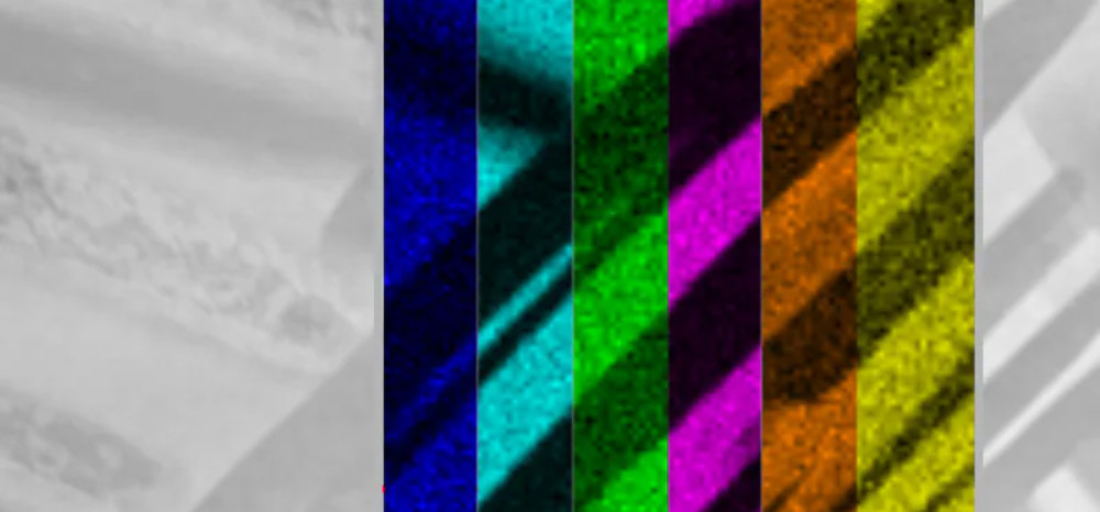
1.2 nm at 500 kV (beam deceleration)Standard Detectors ETD, T1, T2, T3, IR-CCD, Nav-Cam+ ETD, T1, T2, IR-CCD, Nav-Cam+ PivotBeam Selected area electron channel mode (also known as "rocking beam" mode) Not applicable Optional Detectors DBS, LVD, DBS-GAD, STEM 3+, RGB CLD, EDS, EBSD, WDS, Raman, EBIC, etc. ColorSEM Technology (Optional) Real-time quantitative SEM image coloring based on Energy Dispersive X-ray Spectroscopy (EDS).
Includes point & ID, line scan, area, elemental map, and reliable Noran quantification.
Landing Energy Range 20 eV – 30 keV Stage Bias (Beam Deceleration) 4000 V to +600 V standard (per system) Low Vacuum Mode Optional: 10 – 500 Pa chamber pressure. Stage 5-axis motorized eucentric stage, 110 x 110 mm2, 105° tilt range. Maximum sample weight: 5 kg in the untilted position. Maximum Beam Current 50 nA (also configurable to 400 nA) Standard Sample Holder Versatile holder uniquely mounted directly onto the stage, accommodating up to 18 standard sample stubs (Ø12 mm),
three pre-tilted sample stubs, cross-section samples, and two pre-tilted paddle holders (38° and 90°), allowing for tool-free sample mounting.
Chamber 340 mm inner width, 12 ports, up to three simultaneous EDS detectors (two at 180°),
coplanar EDS/EBSD with orthogonal geometry to stage tilt axis
Observation Images:
Palladium nanoparticles imaged using ColorSEM. Frame time: 30 seconds

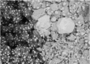
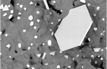
Lithium-ion cathode precursor
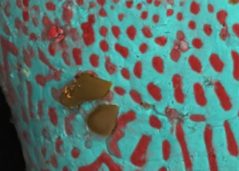
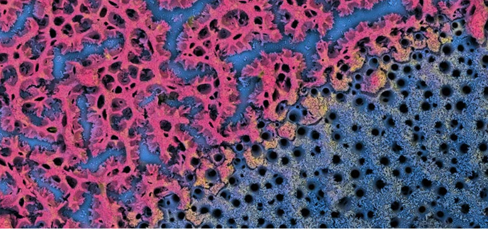
Silver-copper mixture imaged on an Apreo 2 using ColorSEM technology in under a minute and a half.
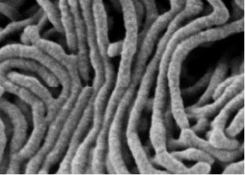
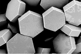
Au/Pd nanoparticles on TiO2 support

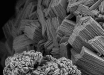
Mixture of polystyrene and polyacrylic acid polymers
Applications:
Fundamental Materials Research
Investigating new materials at ever-smaller scales to maximize control over their physical and chemical properties. Electron microscopy provides researchers with crucial insights into the properties of a wide range of materials from the micron to the nanometer scale.
Quality Control
Quality control and assurance are critical in modern industry. We offer a range of EM and spectroscopy tools for multi-scale and multi-modal defect analysis, enabling you to make reliable, informed
decisions.
Color Scanning Electron Microscopy
ColorSEM technology transforms SEM imaging into a color technique using real-time EDS (Energy Dispersive X-ray Spectroscopy) and real-time quantification. Any user can now continuously acquire elemental data, gaining a more complete picture than ever before.
Energy Dispersive Spectroscopy
Energy Dispersive Spectroscopy (EDS) collects detailed elemental information along with electron microscopy images, providing crucial compositional context to microscopic observations. Using EDS allows for rapid, overall surface scans to individual atoms to determine chemical composition.
Imaging Hot Samples
Studying materials under realistic conditions often requires operation at elevated temperatures. The behavior of materials recrystallizing, melting, deforming, or reacting in the presence of heat can be studied in situ using scanning electron microscopy or DualBeam tools.

Multi-Scale Analysis
New materials must be analyzed at higher resolutions while retaining a larger sample context. Multi-scale analysis allows for the correlation of multiple imaging tools and modalities such as X-ray microCT, DualBeam, focused
ion beam PFIB, SEM, and TEM.
Previous Page
Next Page
Product Inquiry
Welcome to Xiamen Jingwei Instrument Equipment Co., Ltd. Official Website
If you are interested in our products and services, please contact us or leave us a message, and we will be happy to serve you.
Company Address:
(Domestic ):Room 3F-D2, North Rongxin Building, Huli District, Xiamen
(Vietnam ): No. 388, Nguyen Huu Tien Residential Area, Dong Van Ward, Duy Tien Town, Ha Nam Province, Vietnam.
Tel:+86 0592-5631009(Domestic)
Mobile:+86 13859953392(Domestic)
Email:dong5631009@126.com
Tel:+84 0384656346(Vietnam)
Mobile:+84 0384656346(Vietnam)
Email:dongjinzhen9@gmail.com
Quick Navigation:

Mobile Website
Website Construction:www.300.cn | TAG | Privacy policy