

SuperView WX100 white light interferometry probe
Measurement Function: Enables high-precision Z-axis scanning of the sample surface to obtain 3D images. Analysis Function: Enables acquisition of 2D and 3D data regarding surface quality, such as roughness and micro-nano level profile dimensions. Programming Function: Supports pre-configured data processing and analysis tool steps, enabling one-click completion of the entire measurement and analysis process. Batch Analysis: Allows customization of data processing and analysis templates based on required parameters, enabling one-click batch analysis of data with the same type of parameters.
Keywords:
Electronics and Electrical Engineering
Dimension measurement
Product Attachments:
Retail Price
Market Price
Weight
Category:
Remaining Stock
隐藏域元素占位
- Product Description
-
- Commodity name: SuperView WX100 white light interferometry probe
Measurement Function: Enables high-precision Z-axis scanning of the sample surface to obtain 3D images. Analysis Function: Enables acquisition of 2D and 3D data regarding surface quality, such as roughness and micro-nano level profile dimensions. Programming Function: Supports pre-configured data processing and analysis tool steps, enabling one-click completion of the entire measurement and analysis process. Batch Analysis: Allows customization of data processing and analysis templates based on required parameters, enabling one-click batch analysis of data with the same type of parameters.
Product Functions
Measurement Function: Enables high-precision Z-axis scanning of the sample surface to obtain 3D images
Analysis Function: Able to obtain 2D and 3D data such as surface roughness and micro-nano level profile dimensions
Programming Function: Supports pre-configured data processing and analysis tool steps, completing the measurement to analysis process with one click
Batch Analysis: Customizable data processing and analysis templates can be created according to the required parameters to achieve one-click batch analysis for data with the same type of parametersApplication Fields
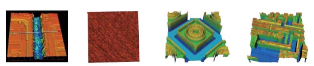
Semiconductors, polished silicon wafers, thinned silicon wafers, wafer ICs
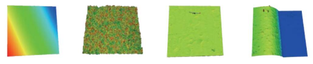
3C electronics, sapphire glass roughness, metal shell mold defects, glass screen height difference
Technical Parameters
Instrument Model
WX110
WX100
Light Source
White LED
Imaging System
1024×1024
Interference Objective
10×,(20×,50×)
Standard Field of View
0.98×0.98mm
Objective Turret
Single Hole
External Dimensions
190×130×350mm
230×200×380mm
Horizontal Adjustment
-
±2° Electric
Z-axis Travel
30mm
Z-axis Scanning Range
10mm (depending on the specific lens)
Z-axis Resolution
0.1nm
Morphology Repeatability
0.1nm
Roughness RMS Repeatability
0.01nm
Step
Accuracy
0.5%
Measurement
Repeatability
0.1%1σ
Product Inquiry
Welcome to Xiamen Jingwei Instrument Equipment Co., Ltd. Official Website
If you are interested in our products and services, please contact us or leave us a message, and we will be happy to serve you.
Company Address:
(Domestic ):Room 3F-D2, North Rongxin Building, Huli District, Xiamen
(Vietnam ): No. 388, Nguyen Huu Tien Residential Area, Dong Van Ward, Duy Tien Town, Ha Nam Province, Vietnam.
Tel:+86 0592-5631009(Domestic)
Mobile:+86 13859953392(Domestic)
Email:dong5631009@126.com
Tel:+84 0384656346(Vietnam)
Mobile:+84 0384656346(Vietnam)
Email:dongjinzhen9@gmail.com
Quick Navigation:

Mobile Website
Website Construction:www.300.cn | TAG | Privacy policy