

SuperView W1 Series Optical 3D Surface Profiler
Optical 3D surface profilometers are instruments used for sub-nanometer level measurement of the surface of various precision devices and materials. Based on the principle of white light interferometry, combined with a precision Z-axis scanning module and 3D modeling algorithms, it performs non-contact scanning of the device surface and establishes a 3D image of the surface. The system software processes and analyzes the 3D image of the device surface, obtaining 2D and 3D parameters that reflect the surface quality of the device, thereby achieving optical detection of the 3D measurement of the device surface topography. SuperView W1 series optical 3D surface profilometers are widely used in semiconductor manufacturing and packaging process detection, 3C electronic glass screens and their precision accessories, optical processing, micro-nano materials and manufacturing, automotive parts, MEMS devices and other ultra-precision processing industries, as well as aerospace, national defense, military industry, and scientific research institutes. It can measure various object surfaces from ultra-smooth to rough, low reflectivity to high reflectivity, roughness, flatness, microscopic geometric profile, curvature, etc., of workpieces from nanometer to micrometer level, providing more than 300 2D and 3D parameters based on four domestic and international standards including ISO/ASME/EUR/GBT as evaluation standards.
Keywords:
Dimension measurement
Electronics and Electrical Engineering
Product Attachments:
Retail Price
Market Price
Weight
Category:
Remaining Stock
隐藏域元素占位
- Product Description
-
- Commodity name: SuperView W1 Series Optical 3D Surface Profiler
Optical 3D surface profilometers are instruments used for sub-nanometer level measurement of the surface of various precision devices and materials. Based on the principle of white light interferometry, combined with a precision Z-axis scanning module and 3D modeling algorithms, it performs non-contact scanning of the device surface and establishes a 3D image of the surface. The system software processes and analyzes the 3D image of the device surface, obtaining 2D and 3D parameters that reflect the surface quality of the device, thereby achieving optical detection of the 3D measurement of the device surface topography. SuperView W1 series optical 3D surface profilometers are widely used in semiconductor manufacturing and packaging process detection, 3C electronic glass screens and their precision accessories, optical processing, micro-nano materials and manufacturing, automotive parts, MEMS devices and other ultra-precision processing industries, as well as aerospace, national defense, military industry, and scientific research institutes. It can measure various object surfaces from ultra-smooth to rough, low reflectivity to high reflectivity, roughness, flatness, microscopic geometric profile, curvature, etc., of workpieces from nanometer to micrometer level, providing more than 300 2D and 3D parameters based on four domestic and international standards including ISO/ASME/EUR/GBT as evaluation standards.
Product Introduction
The optical 3D surface profiler is a detection instrument used for sub-nanometer-level measurement of the surface of various precision devices and materials. Based on white light interference technology, combined with a precision Z-axis scanning module and 3D modeling algorithms, it performs non-contact scanning of the device surface to establish a 3D surface image. The system software processes and analyzes the 3D image of the device surface, obtaining 2D and 3D parameters that reflect the surface quality of the device, thus achieving optical detection of the 3D measurement of the device surface morphology.
The SuperView W1 series optical 3D surface profiler can be widely used in semiconductor manufacturing and packaging process detection, 3C electronic glass screens and their precision accessories, optical processing, micro-nano materials and manufacturing, automotive parts, MEMS devices and other ultra-precision processing industries, as well as aerospace, national defense, military industry, and scientific research institutes. It can measure various object surfaces, from ultra-smooth to rough, low reflectivity to high reflectivity, and the roughness, flatness, micro-geometric profile, curvature, etc., of workpieces from the nano to micron level, providing over 300 types of 2D and 3D parameters based on four domestic and international standards (ISO/ASME/EUR/GBT) as evaluation standards.
Product Functions
1) The equipment provides functions for measuring profile dimensions such as roughness, step height, and angle that characterize micro-morphology;
2) Automatic focusing, automatic fringe finding, and automatic brightness adjustment are provided during measurement;
3) Automatic stitching measurement and automatic multi-area measurement positioning functions are provided during measurement;
4) Four modules of data processing functions are provided in the analysis, including leveling, image scanning, noise reduction and filtering, and region extraction;
5) Five analysis functions are provided in the analysis, including roughness analysis, geometric profile analysis, structural analysis, frequency analysis, and function analysis;
6) One-click analysis and multi-file analysis auxiliary analysis functions are provided simultaneously in the analysis.Application Fields
Measurement and analysis of surface morphology characteristics such as planarity, roughness, waviness, surface profile, surface defects, wear, corrosion, pore gaps, step height, bending deformation, and processing conditions of various product surfaces, components and materials.
Application Examples:
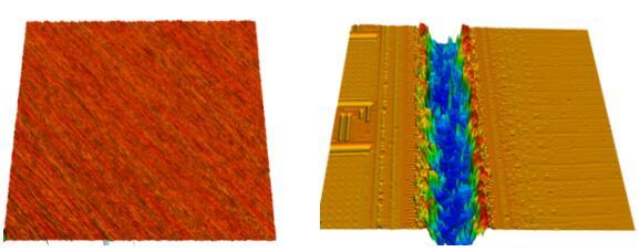
Semiconductor manufacturing (thinning roughness, laser groove profile)
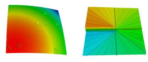
Optical components. Curvature & profile dimensions & roughness
(Ultra-precision) Machining. Profile dimensions & angle
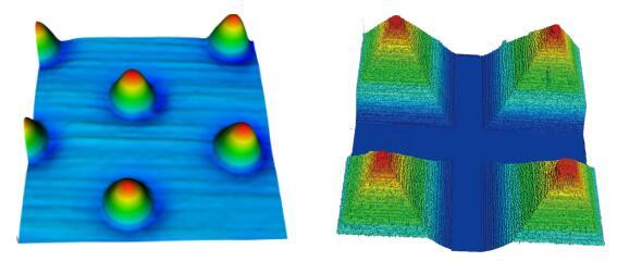
Surface engineering (tribology) Profile area & volume
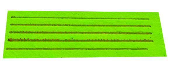
3C electronics (glass screen) Roughness
Standard block. Step height & roughness
Performance Features
1. High precision, high repeatability
1) The measurement system consists of optical interference technology, a precision Z-axis scanning module, and an excellent 3D reconstruction algorithm, ensuring high measurement accuracy;
2) The unique vibration isolation system effectively isolates most vibrations above 2Hz, eliminating ground vibration noise and airborne acoustic vibration noise, ensuring that the instrument can be used stably in most production workshop environments and obtaining extremely high measurement repeatability;2. Environmental noise detection function
Equipped with an environmental noise detection module with 0.1nm resolution, it can quantitatively evaluate the vibration interference of the external environment on the instrument's scanning axis, providing quantitative environmental noise data as support during equipment debugging, daily monitoring, and troubleshooting.3. Precision operating handle
The integrated operating handle with X, Y, and Z directional displacement adjustment functions can quickly complete the pre-measurement work such as sample stage translation, Z-axis focusing, and fringe finding.4. Dual collision protection measures
In addition to the primary software ZSTOP setting Z-axis displacement lower limit for collision protection, a mechanical electronic sensor is also designed on the Z-axis. When the lens touches the sample surface, the instrument automatically enters an emergency stop state, maximizing the protection of the instrument and reducing the risk of human operation.5. Dual-channel air-floating vibration isolation system
It can connect to the customer's on-site stable air source or the standard-equipped quiet air compressor, allowing stable operation even without an external air source.Technical Specifications
1. Technical Specifications Table
Model W1 W1-Pro W1-Ultra WM100 Light Source White LED Imaging System 1024×1024 Interference Objective Standard: 10×
Optional: 2.5×, 5×, 20×, 50×, 100×
Optical ZOOM Standard: 0.5×
Optional: 0.375×, 0.75×, 1×Standard: 0.5×
Optional: 0.375×, 0.75×Standard Field of View 0.98×0.98㎜ (10× objective, 0.5× optical ZOOM) Objective Turret Standard: 3-hole manual
Optional: 5-hole electric
5-hole electric XY Stage Dimensions 320×200㎜ 300×300㎜ 320×200㎜ 220×220mm Travel Range 140×100㎜ 200×200㎜ 140×100㎜ 100×100 mm Load 10kg Control Method Electric Horizontal Adjustment ±5° ±3° Z-axis Focusing Travel 100㎜ 50㎜ Control Method Electric Z-axis Scanning Range 10 ㎜ Morphology Repeatability STR*1 0.1nm Roughness RMS Repeatability*2 0.005nm 0.01nm Step Measurement*3 Accuracy: 0.3%; Repeatability: 0.08%(1σ) Accuracy: 0.5%; Repeatability: 0.1%(1σ) Scanning Speed at 0.1nm Resolution 1.85μm/s 1.85μm/s 8μm/s 1.85μm/s Instrument Host Weight <160㎏ 50㎏ Host Dimensions (Length×Width×Height) 700×606×920㎜ 440×330×700㎜ Environmental Conditions Operating Temperature 15℃ ~30℃, Temperature Gradient < 1℃/15 minutes Relative Humidity 5%-95%RH, Non-condensing Environmental Vibration VC-C or better Software Monitoring Noise*4 3σ≤4nm Vibration Isolation Air Source 0.6Mpa stable and clean air source, oil-free, water-free, air tube diameter 6㎜ (air source optional) Power Supply 100-240VAC, 50/60Hz, 4A, 300W Other No strong magnetic field, no corrosive gases Note:
*1 Measured Sa of 0.2nm silicon wafer with single fringe and 80μm full field filter in EPSI mode under laboratory conditions.
*2 Roughness performance parameters are obtained based on ISO 25178 international standard by measuring Sa of 0.2nm silicon wafer RMS parameters under laboratory conditions.
*3 Step height performance parameters are obtained based on ISO 10610-1:2009 standard by measuring 4.7µm step height standard block under laboratory conditions.
*4 When the equipment software noise evaluation is 4nm≤3σ≤10nm, the roughness RMS repeatability is revised to 0.015nm, the step height accuracy is revised to 0.7%, and the step height repeatability is revised to 0.12%; when the software noise evaluation is 3σ>10nm, the environment does not meet the equipment usage requirements, and the site needs to be changed.
Product Inquiry
Welcome to Xiamen Jingwei Instrument Equipment Co., Ltd. Official Website
If you are interested in our products and services, please contact us or leave us a message, and we will be happy to serve you.
Company Address:
(Domestic ):Room 3F-D2, North Rongxin Building, Huli District, Xiamen
(Vietnam ): No. 388, Nguyen Huu Tien Residential Area, Dong Van Ward, Duy Tien Town, Ha Nam Province, Vietnam.
Tel:+86 0592-5631009(Domestic)
Mobile:+86 13859953392(Domestic)
Email:dong5631009@126.com
Tel:+84 0384656346(Vietnam)
Mobile:+84 0384656346(Vietnam)
Email:dongjinzhen9@gmail.com
Quick Navigation:

Mobile Website
Website Construction:www.300.cn | TAG | Privacy policy